Sony Corporation Global Headquarters
Global
Sony Corporation Global Headquarters

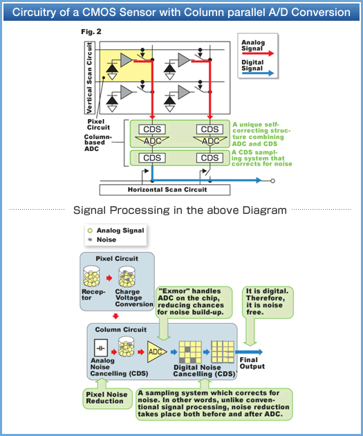
Sony developed CMOS Sensor "Exmor", which adopts the "Column-Parallel A/D Conversion Technique" to create images containing more detail than ever before. It combines the speed of the CMOS sensor with advanced-quality image sensor technologies accumulated through the development of CCDs. The result is enhanced resolution along both the space and time axes. With these innovations, Sony is exploring the limitless potential of the world of imaging.
A high-speed imaging sensor must combine high-sensitivity with low noise. In a CMOS sensor, the pixels, signal readout circuit, analog-to-digital conversion circuit and controller are all built into a single chip. By optimizing the composition and operation of each circuit, Sony has achieved previously incompatible goals of increasing both speed and image quality.